Week. Applications and Implications#
- Author : kai naito / Asako Okazaki(Fablab Kamakura)
- Date created : 04/11/2019
- modified: 4/4/2020
- modified: 5/14/2021 by Kae Nagano
Time table#
-
5.20(Thu) 20:00-21:00
- Global session review
- Review assignments
- Final Project/ Nueval
- Q&A
-
5.22(Sat) 10:00-18:00
- Indivisual work (Final Project)
Assignments#
- Refer to Assessment page
Group assignment#
- No Group aaignment
Individual Assignments#
- Propose a final project masterpiece that integrates the range of units covered, answering:
- Your project should incorporate 2D and 3D design,
- additive and subtractive fabrication processes,
- electronics design and production,
- embedded microcontroller interfacing and programming,
- system integration and packaging
- Where possible, you should make rather than buy
- the parts of your project
- Projects can be separate or joint, but need to show individual mastery of the skills, and be independently operable
Learning outcomes#
- Define the scope of a project
- Develop a project plan
Have you answered these questions??#
- What will it do? 何をするものなのか?
- Who’s done what beforehand? 先行のプロジェクト
- What will you design? 新しく自分がデザインする部分は?
- What materials and components will be used? 材料と部品
- Where will come from? 材料と部品の仕入先
- How much will they cost? 材料と部品の金額
- What parts and systems will be made? 制作するもの
- What processes will be used? 制作方法(additive / subtractive両方使うこと)
- What questions need to be answered? 現状の課題
- How will it be evaluated? プロジェクトのゴールと評価基準
The answers to the questions above will allow you to create your BOM (Bill Of Materials).
Advices from Instructors#
-
Goal for the week
- To determine and document the specifications for the Final Project.
- Final Projectの仕様を決定してドキュメンテーションする。
-
Advice
-
It’s okay if things change later, so please apply the current plan to the requirements and put them together.
- あとから変わっても構わないので、現時点のプランを要件に当てはめてまとめてください。
-
The BOM (bill of materials) is OK that you are planning as of today.
- BOM(bill of materials : 材料リスト)は、現時点でわかっているものでOK。
-
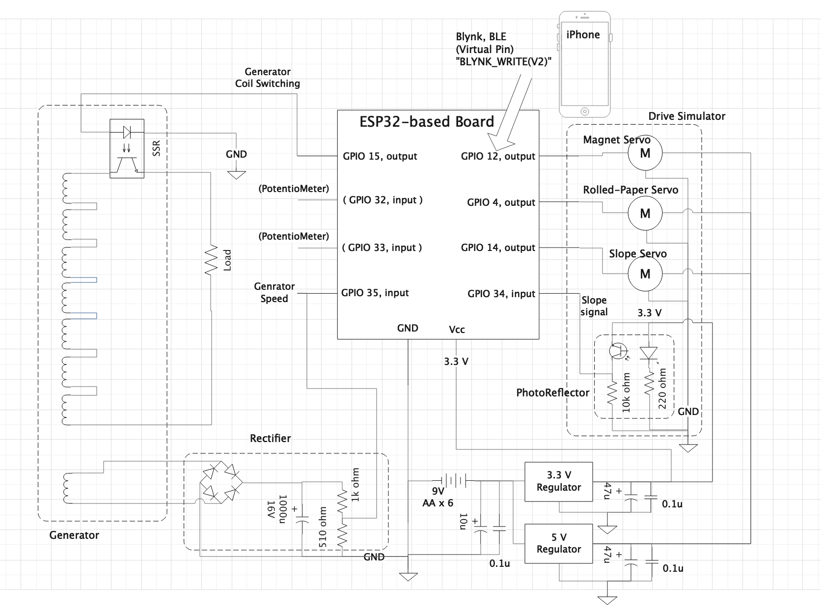
It is recommended to draw a simple “system diagram” and “flowchart”.
-
簡単な「システム図」と「フローチャート」を書くことをお勧めします。
-
e.g.)System diagram

-

- 例)フローチャート

-
Requirements of Final project#
- Read carefully Final Project Requirements
- Commercial Board Policy
Learning outcomes#
- Create your own integrated design
- Demonstrate 2D & 3D modelling capabilities applied to your own designs
- Select and apply appropriate additive and subtractive techniques
- Demonstrate competence in design, fabrication and programming of your own fabbed microcontroller PCB, including an input & output device
Have you answered these questions?#
- Made your slide> 1920 x 1080 pixels with your name, project name, Fab Lab name, a photo/render/sketch of your project, a brief description of what your project is/does
- Made a ~1 minute (10MB/1080p) video of you explaining your project
- Made a separate Final Project page that briefly summarises your project
- Included the BOM (Bill of Materials) for your project
- Linked from this page to any weeks that you worked on your final project
- Linked to your presentation.png and presentation.mp4
- Included all of your original design files in the archive (2D & 3D, board files & code). No external hosting of final project files - discuss file sizes with your instructor
- Included the license you chose
- Acknowledged work done by others
- プロジェクトの要件:
- Additiveとsubtractiveファブリケーションプロセスを含むこと
- エレクトロニクスを含むこと
- マイクロコントローラーのボードを含むこと
- input deviceとoutput deviceを含める
- (可能なら)モジュールを買うのではなく、自分で作ること
- 自分のrepoに全てのデータを格納する
Announcements / notes#
Recitation#
No recitation this week.
Schedule#
-
Final presentations
- ~200 students, 180 min/session, 50/session
- Wed Jun 09
- Fri Jun 11
- Mon Jun 14
- Wed Jun 16
- (Fri Jun 18, hold if needed)
-
Cutoff
- June 21: local to global eval cutoff
- July 5: global eval to student cutoff
- July 12: global eval to FAB16 graduation cutoff
- Aug 9-13: FAB16
- Dec 1: post-FAB16 cutoff for this cycle