KiCad tutorial#
- Author : Jun Kawahara (FabLab Kamakura)
- Date created : 2021/03/11
- Environment
- macOS Mojave 10.14.6
- KiCad 5.1.5-0-10_14
KiCad is an open source software suite for Electronic Design Automation (EDA). The programs handle Schematic Capture, and PCB Layout with Gerber output.
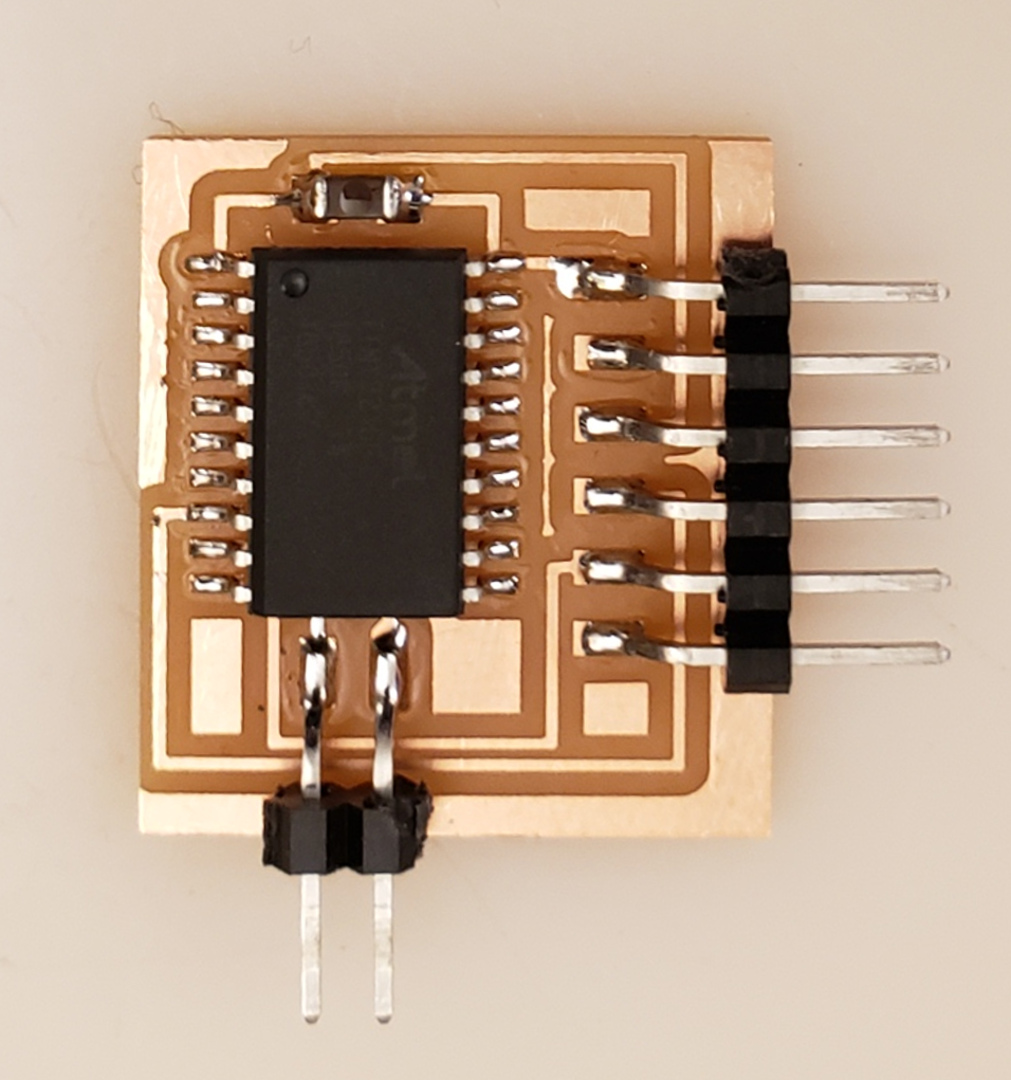
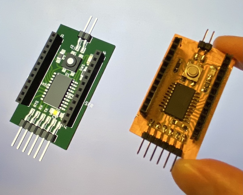
I’ll explain how to handle with KiCad in the context of Electronics Design in Fab Academy. Let us redraw Neil’s hello.t3216.echo board with more breakout pins, an LED and a button.
KiCad Workflow#
If you are migrating from Eagle to KiCad, you might be confused by its workflow. I’ll explain based on following steps.
- install, launch KiCad and add a fab library
- create a project
- Eeschema
2.1 add components
2.2 annotate components
2.3 electrical rule check(ERC)
2.4 associate components with footprints(CvPcb)
2.5 generate netlist - Pcbnew
3.1 import netlist
3.2 design PCB
3.3 design rule check(DRC)
3.4 export images for milling - mods settings
0. install, launch KiCad and add fab library#
Download KiCad, install and launch it.
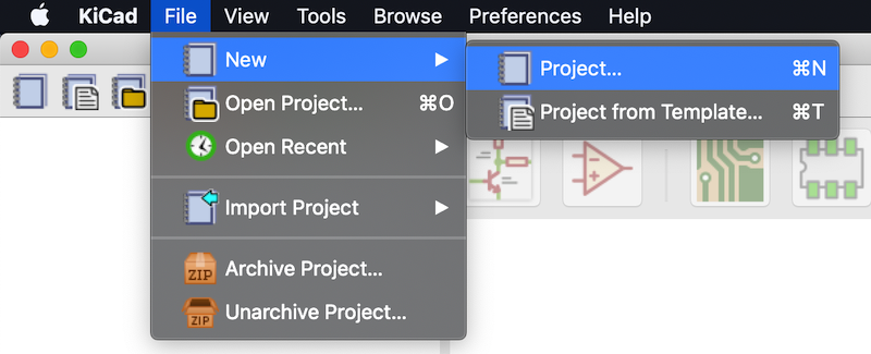
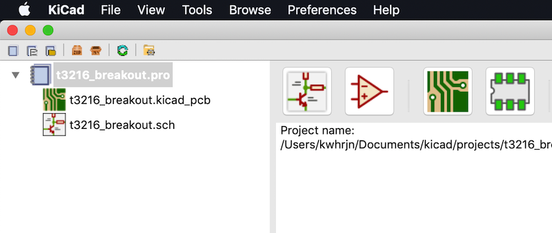
File > New > Project…
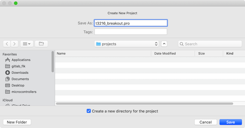
Enter a project name, remain checked “Create a new directory for the project,” and click Save.
It will create .sch and .kicad_pcb files.
1. add a fab library#
Download/unzip or clone Fab electronics component library for KiCad from fabcloud, or from a repo of CBA.
digikey-kicad-library is also useful. A link to how to install the library.
If you clone the repo, a folder kicad will be created. If you download a zip file and unzip it, a folder kicad_master will be created. Move the folder to your KiCad library folder so you can use it later, and rename the folder name if you want to.
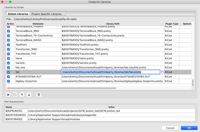
For example, I stored it under a folder, /Users/yourusername/Documents/kicad/thirdparty_libraries/, and renamed it fab.
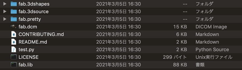
The folder contains following files and folders. You have to point paths to fab.lib as a symbol library, and to fab.pretty as a footprint library.
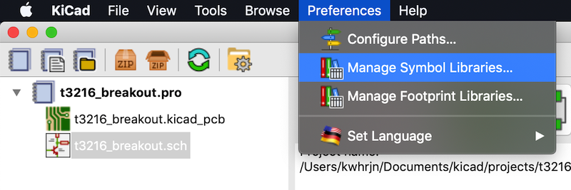
Open Preferences > Manage Symbol Libraries…
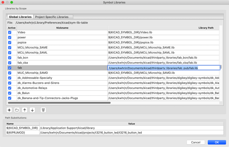
 Click a plus button of the bottom left corner. input a nickname, (here, fab), and navigate to a folder containing fab.lib.
Same as above, select Preferences > Manage Footprint Libraries…, fab as nickname, and navigate to fab.pretty folder.
All set! Now make your own PCB with KiCad!!!
2. Eeschema#
2.1 add components#
Open .sch file. Eeschema, as its name tell, is a schematic editor. In adding symbols, it is a quite useful to use hotkeys. If you press Command + F1 key, hotkey list will show up. You don’t learn by heart all of them soon, but here is some often-used hotkeys.
| hotkeys | description |
|---|---|
| A | Add a new symbol to the sheet |
| R | Rotate |
| M | Move (wires will be disconnected) |
| G | Grab and move a symbol while keeping wires connected |
| L | add a Label |
| W | Start drawing a Wire |
| V | edit Value |
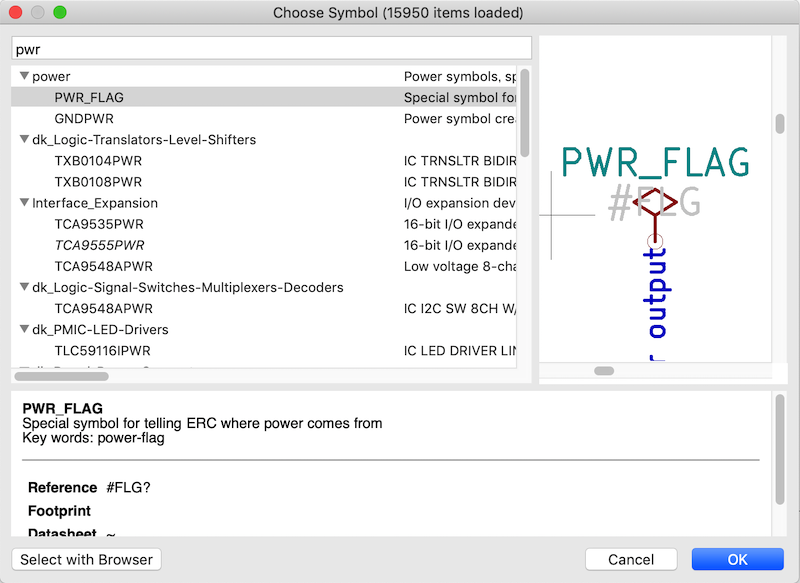
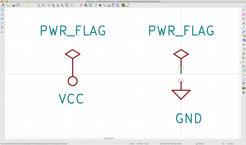
The first component to add is PWR_FLAG. KiCad wants to know where the power (and GND) come from. In order to do so, PWR_FLAG symbol is used.
Press A for add a component, or click ![]() and click again on the sheet. Choose Symbol window will show up.
and click again on the sheet. Choose Symbol window will show up.
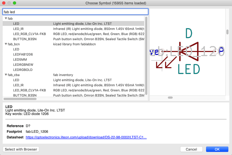
Search pwr_flag, hit OK and place it on your schematic sheet.
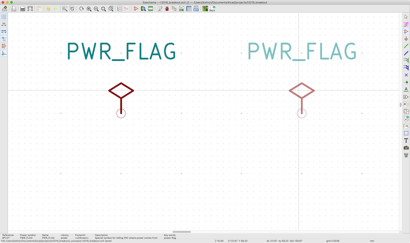
Press C on a PWR_FLAG symbol to copy it, move a half-transparent copied symbol and place it on the schematic sheet.
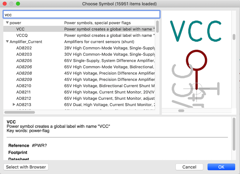
Press A and search vcc,
and if you press R, the component will rotate by 90 degrees
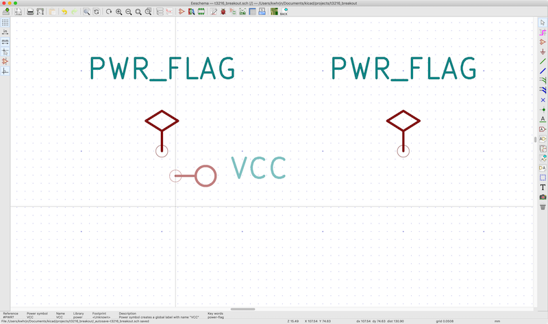
Click when each circle of symbols overlaps
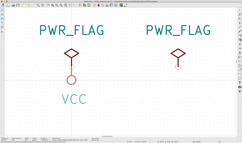
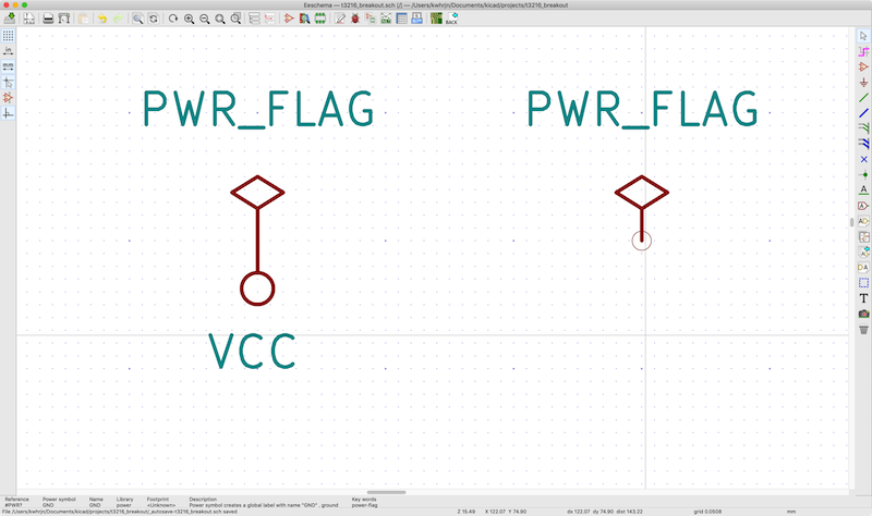
Add GND symbol.
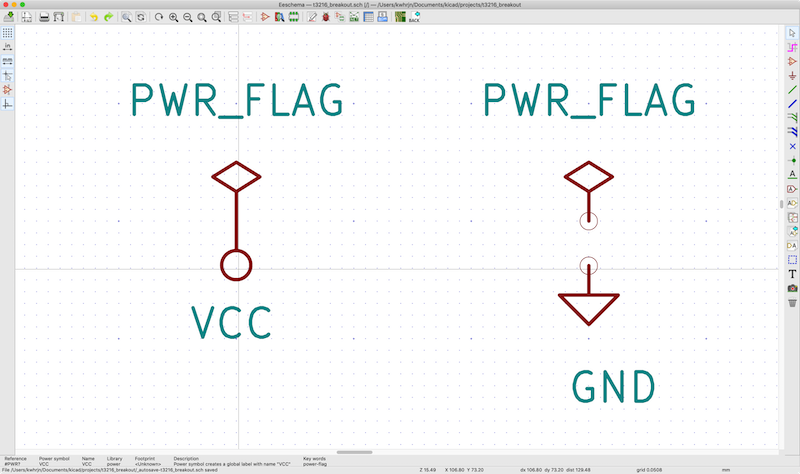
Place the cursor in the middle of a circle of a symbol, and Press R. Wiring starts.
Place the cursor in the middle of a circle of a symbol to which you want to connect wire, then click.
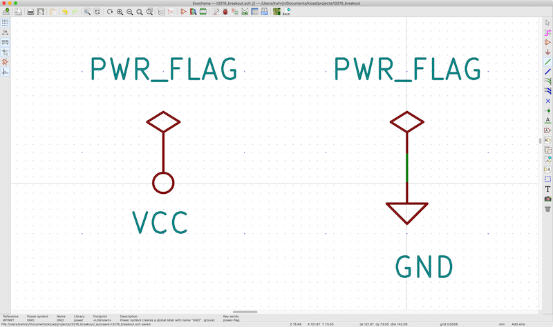
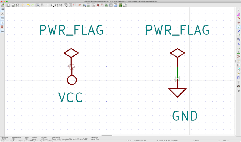
If symbols look like this, they are bad connections.
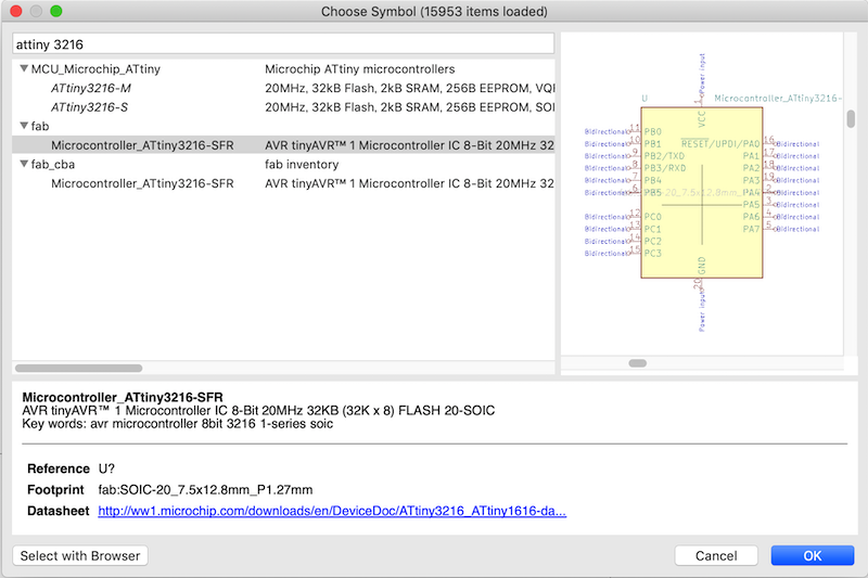
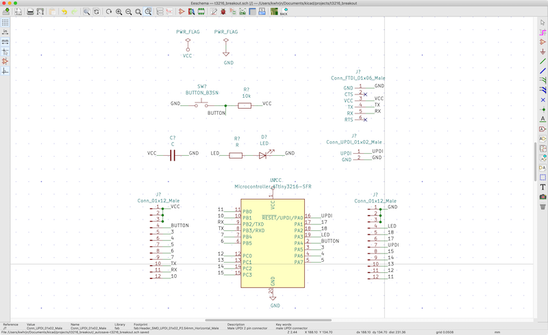
2.1.1 ATtiny3216#
Press A, search and addattiny 3216.
Add VCC onto pin 1, and GND to pin 20. Also connect wires to each pin.
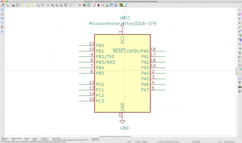
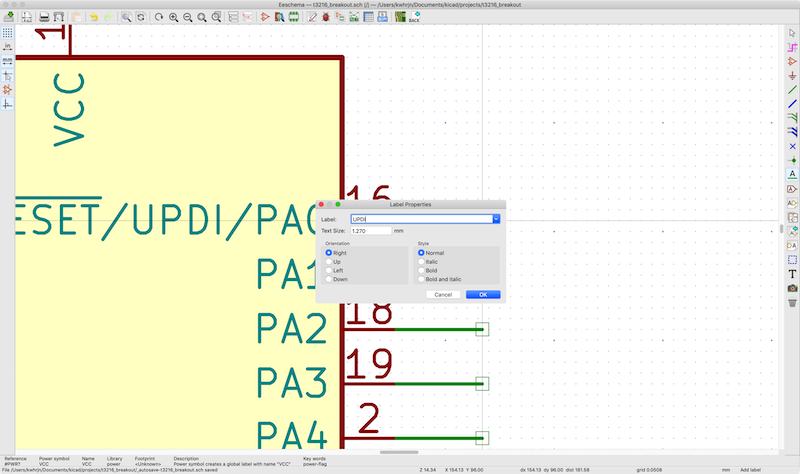
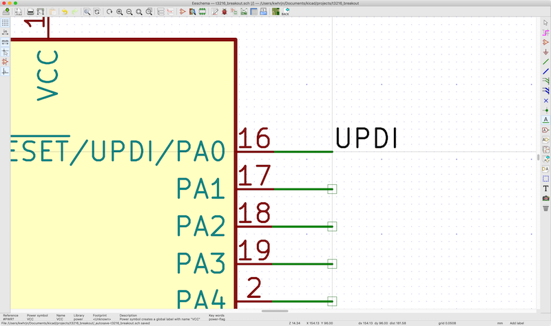
Label wires. Place cursor in the middle of a square of a wire, press L and Label Properties window will show up. Input label name, and KiCad connects labels with the same name.
For example, pin 16 is for UPDI programming pin, so label it UPDI.
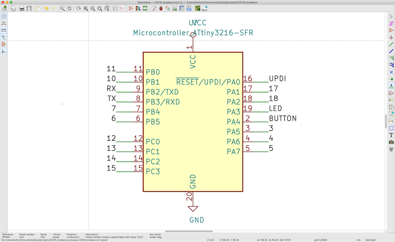
Do as the same for other pins like below.
2.1.2 pinheaders#
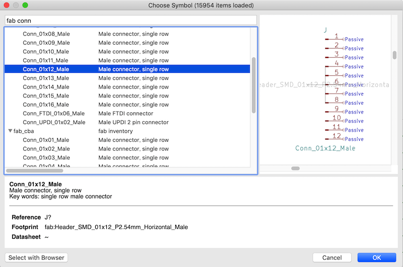
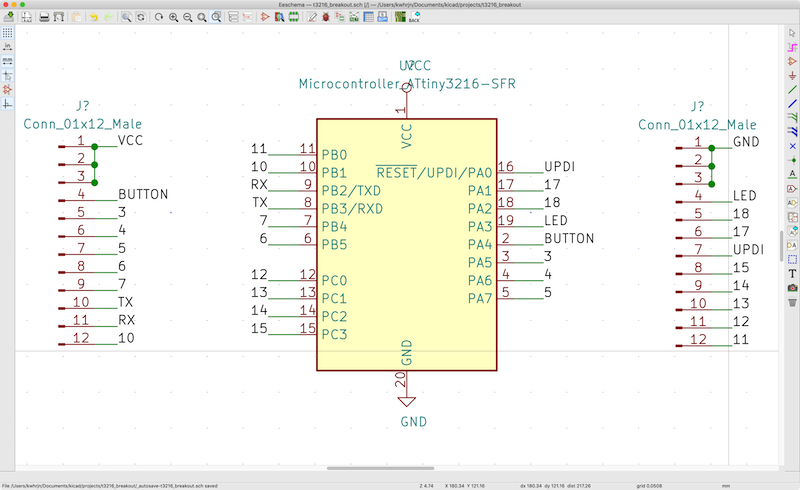
Next, pinheaders for ATtiny 3216 breakout board. Search fab conn. I selected 12 pins in a single row. ATtiny 3216 has 20 pins, so 10-pin connector is enough, but I choose it because I want additional pins for VCC and GND.
Connect wires to each pin and label them like below.
2.1.3 a bypass condenser, LED#
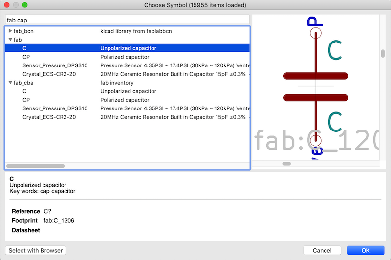
Search fab cap, add an unpolarized capacitor for a bypass capacitor.
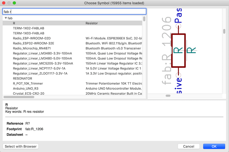
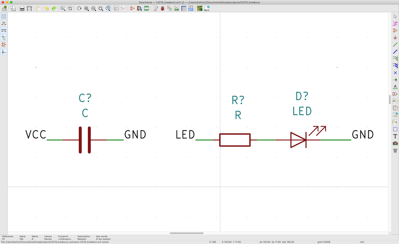
Search and add fab r for a register, and fab led for an LED
Draw Wires and label them like below.
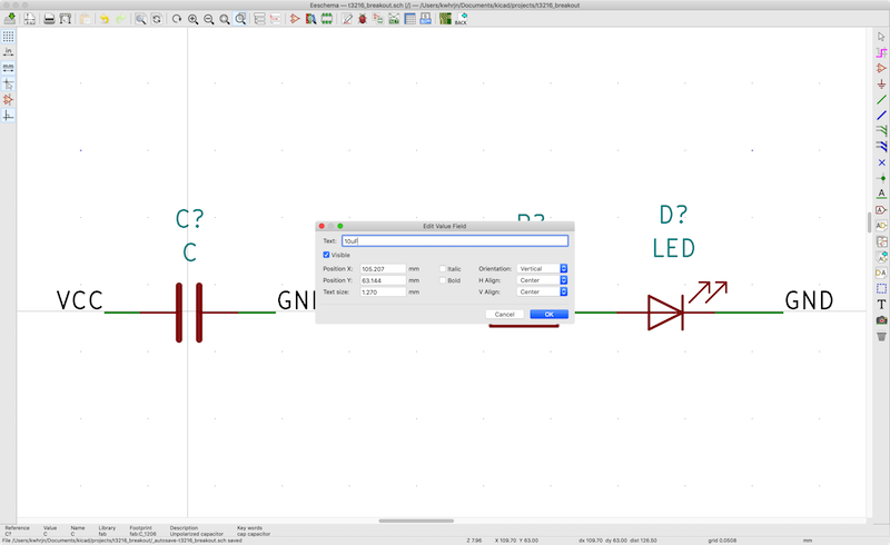
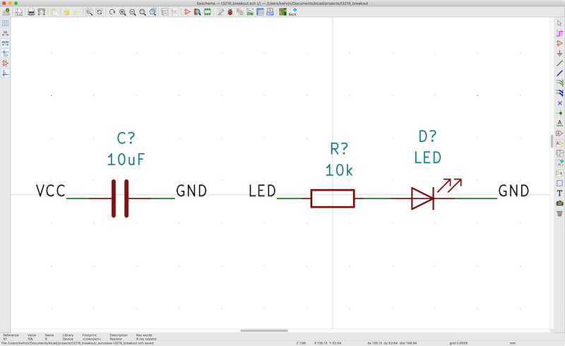
Place the cursor on a symbol(for example, a capacitor), and press V. Input the value of it, here 10 uF.
Also input a register value, 10k ohm.
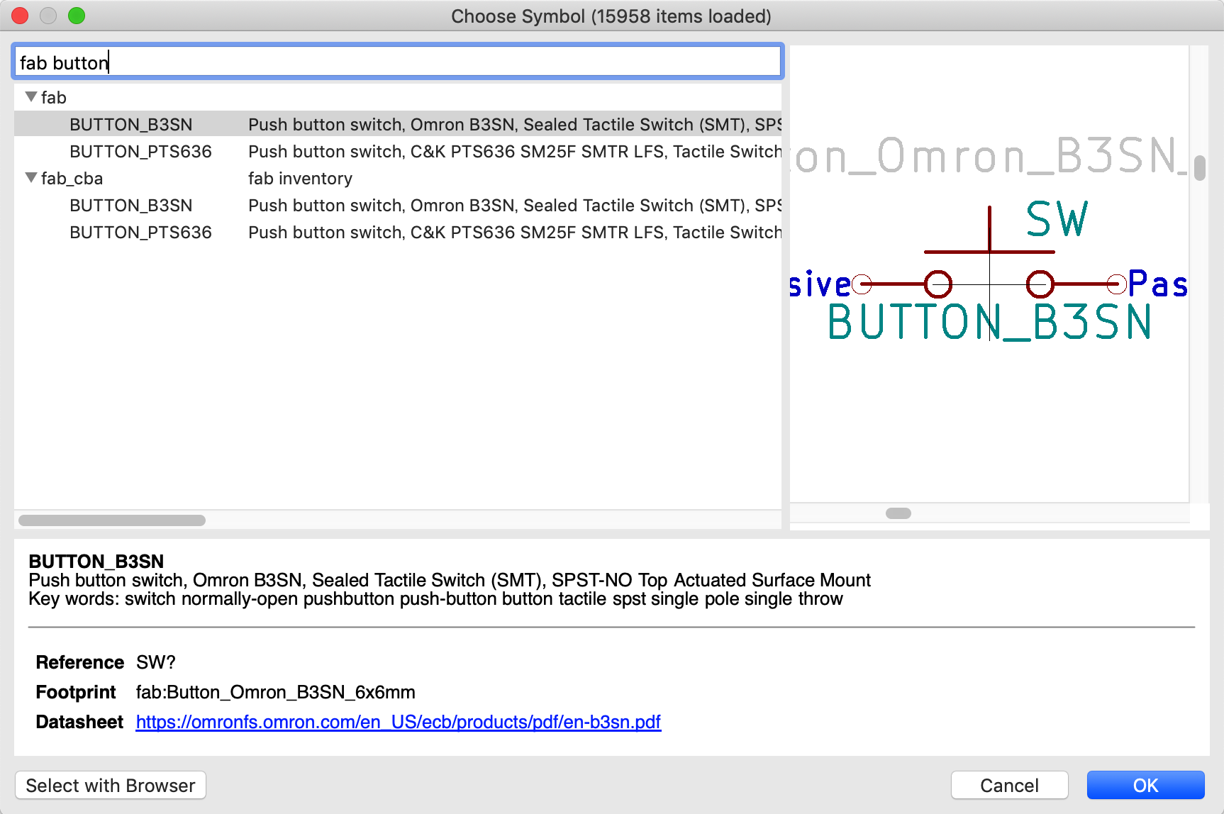
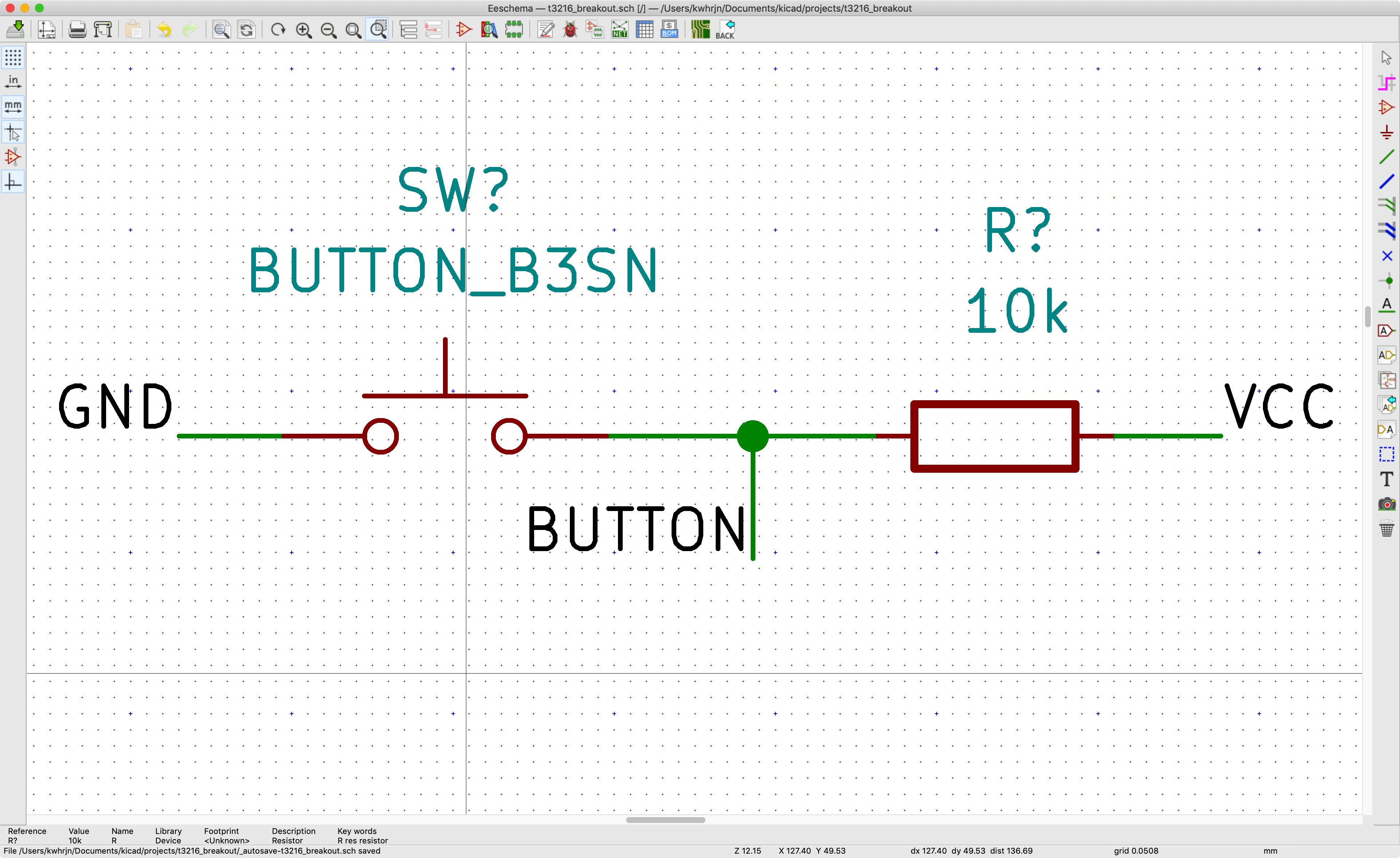
2.1.4 a button and a pull-up register#
Search fab button, select and add BUTTON_B3SN.
Add a pull-up register. Draw wires and label them. Also edit the register value, 10k.
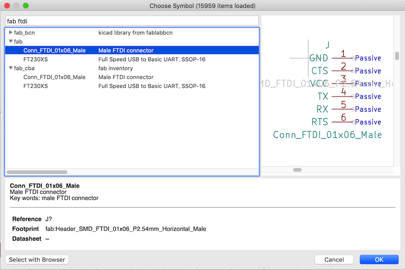
2.1.5 FTDI connector#
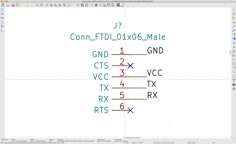
Search fab ftdi, select and add Conn_FTDI_01x06_Male.
Draw wires and label them. In KiCad, you have to place no connection flag ![]() onto unused pins.
onto unused pins.
2.1.6 UPDI connector#
Search fab updi, select and add Conn_UPDI_01x02_Male.
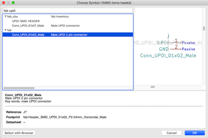
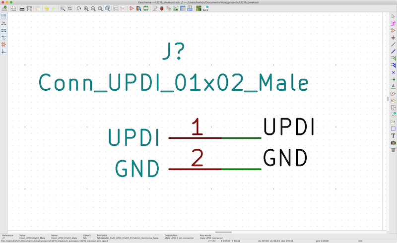
Draw wires and label them like below.
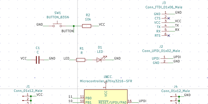
Now you’ve added all symbols. Well done!
2.2 annotate components#
If you look at your schematic closely, you’ll notice components are not annotated, such as U?, SW?, R?, J?.
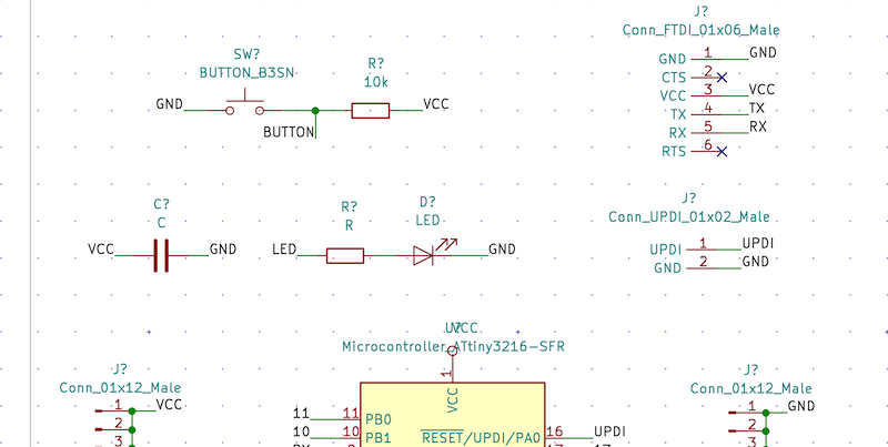
Open annotation tool to give components references.
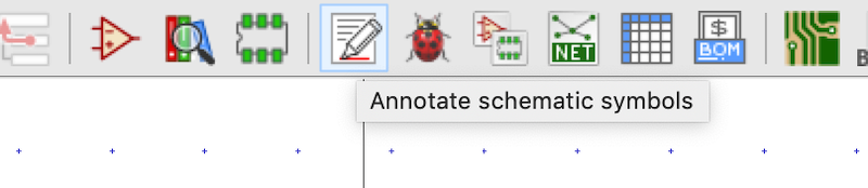
Click Annotate button, and some messages will show. Close the window.
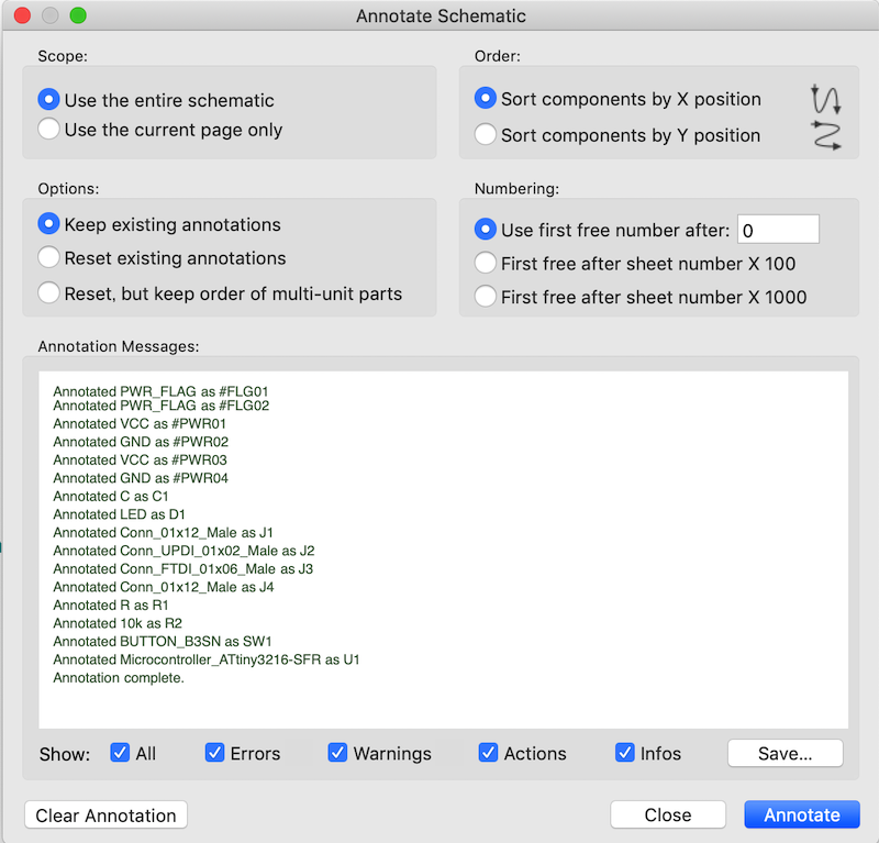
Components are now annotated.
2.3 electrical rule check(ERC)#
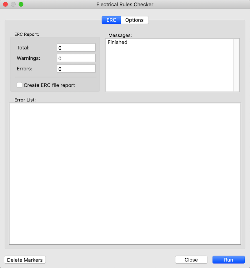
Run ERC to check the continuity in your schematics. Click a ladybug icon to open Electrical Rules Checker.
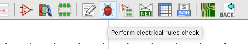
Click Run. In this design, there’re no warnings and errors. If you have some of them, please reexamine your schematic before you go on to the next step.
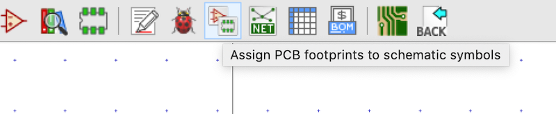
2.4 associate components with footprints(CvPcb)#
If you are familiar with Autodesk Eagle, a schematic symbol is associated with a footprint. If you want to make your PCB with THT(Through-Hole Technology) or SMD(Surface-mount Device), you have to choose a symbol corresponding footprints.
In KiCad, you can associate footprints with components with CvPcb.
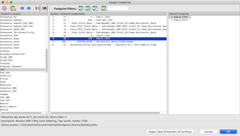
In fab library, footprints are already associated with symbols, except resistors. Here’s an example how to assign a footprint to a symbol.
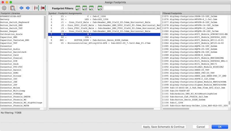
In the center pane, choose a component to which you want to assign a footprint, and in the left pane choose fab library. There are still a lot of options in the right pane.
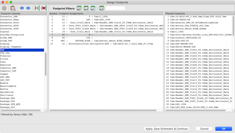
Activate a filter by pin count, it shows only footprints that have the same number of pads as the symbol has.
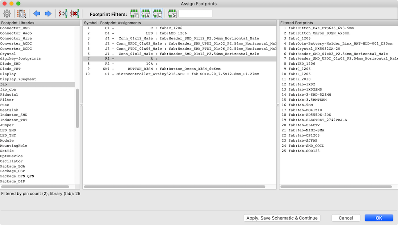
If you use a filter by the symbols footprint, it will narrows down the options. It makes easier for you to find a footprint you want. Double clicking fab:R_1206 in the right pane will assign the footprint to the symbol.
Do as the same to another resistor.
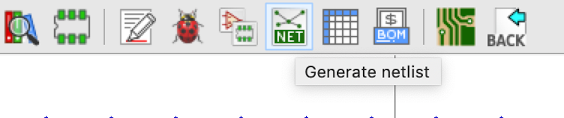
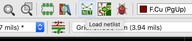
2.5 generate netlist#
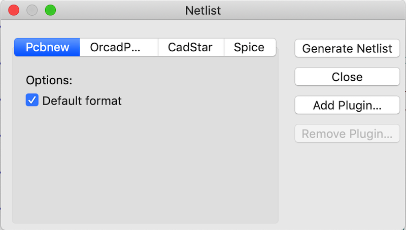
Now you assigned footprints to all symbols, and your work in Eeschema is almost done. Before doing layout in Pcbnew, one thing you have do is to export netlist. Netlist is, according to the document of KiCad,
A netlist is a file which describes electrical connections between symbols. These connections are referred to as nets. In the netlist file you can find:
- The list of the symbols - The list of connections (nets) between symbols.
Click Generate netlist icon
Just press Generate Netlist button, and save the netlist file(.net), usually in the present project folder.
3. Pcbnew#
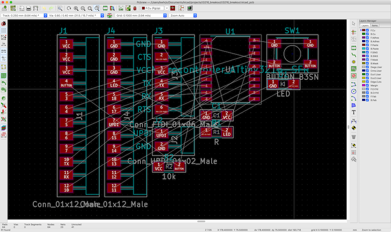
3.1 import netlist#
Open Pcbnew
Import netlist file that was exported from Eeschema before.
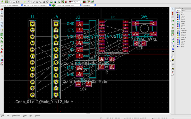
These are footprints you have to layout in your PCB.
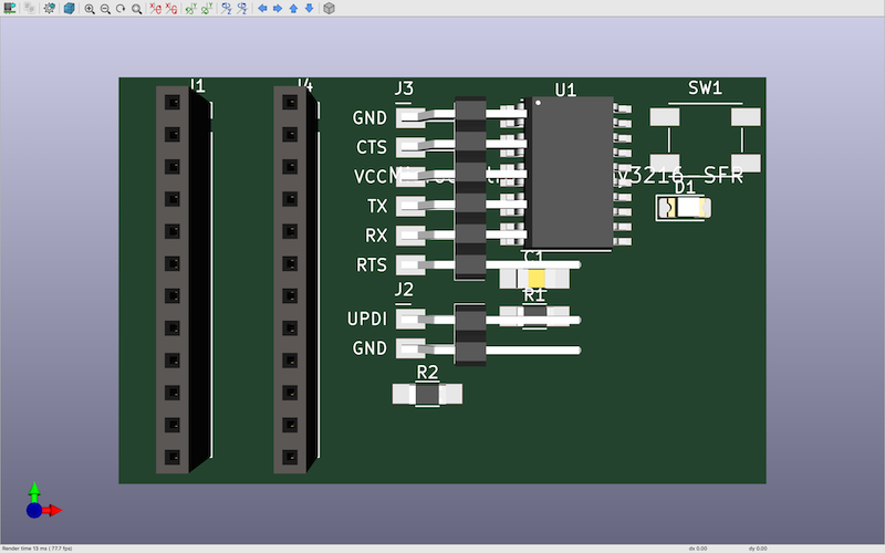
Try, Pcbnew > View > 3D Viewer. That will show you 3D rendering of your board. It helps you know what your board design is going to be like before milling.
You’ll notice that a footprint assigned to an LED and a button doesn’t have 3D model. Also, 01x12 breakout are male horizontal pinheaders(that’s my mistake).
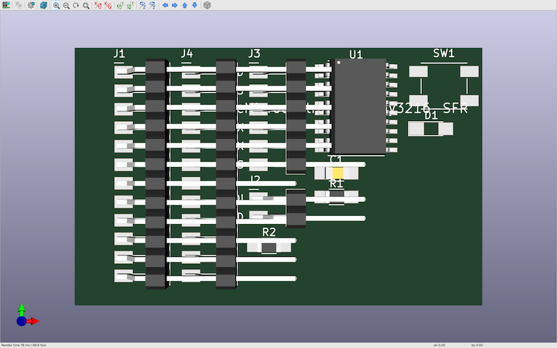
As an exercise, let’s go back to Cvpcb, and assign other footprint to 01x12 pinheaders and an LED. Also I’ll show you how to addd 3D model to a button footprint.
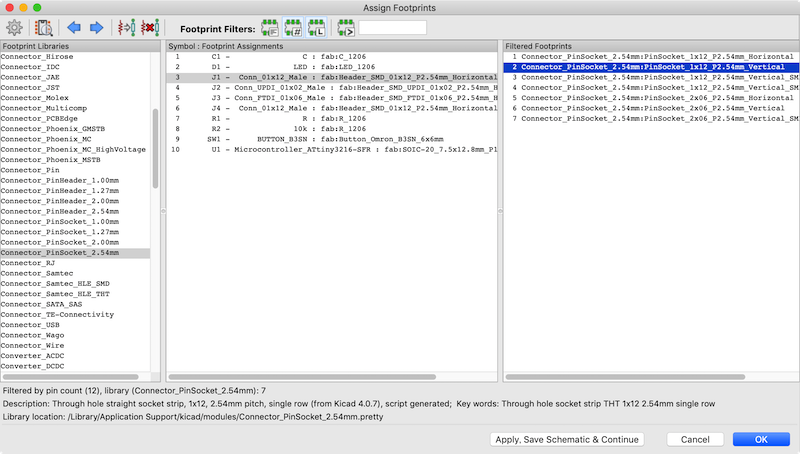
3.1.1 01x12 socket, and an LED#
Back to Eescchema, and open Cvpcb.
Select J1(your reference might not be the same) in the center pane, Connector_PinSocket_2.54mm library in the left pane, activate a filter by pin number. Apply PinSocket_1x12_P2.54mm_Vertical in the right pane.
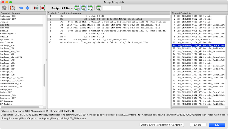
Next, LED. Select D1(yours might not be the same) in the center pane, LED_SMD library in the left pane, activate a filter by pin number. Apply LED_1206_3216Metric_Castellated in the right pane.
Export netlist, and import it again with Pcbnew. KiCad will tell changes applied to PCB, and click Update PCB.
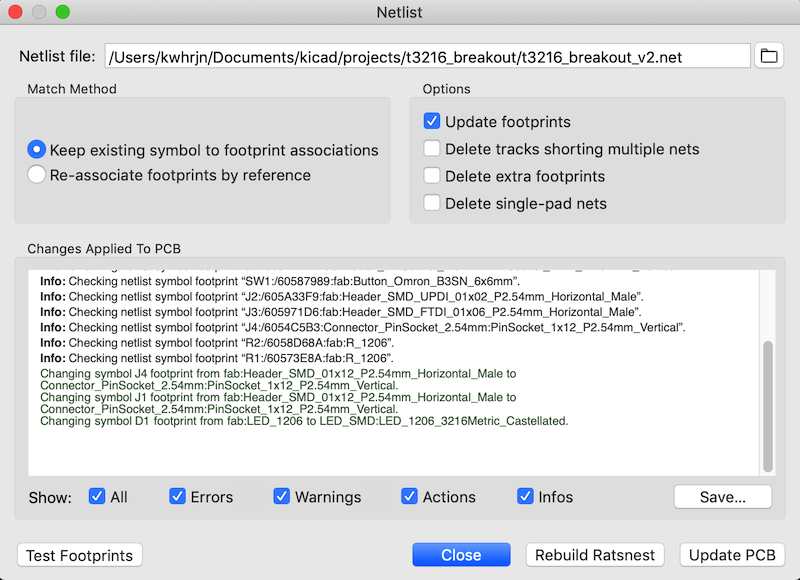
Pinheaders are changed to sockets.
In 3D viewer, the LED has now 3D rendering.
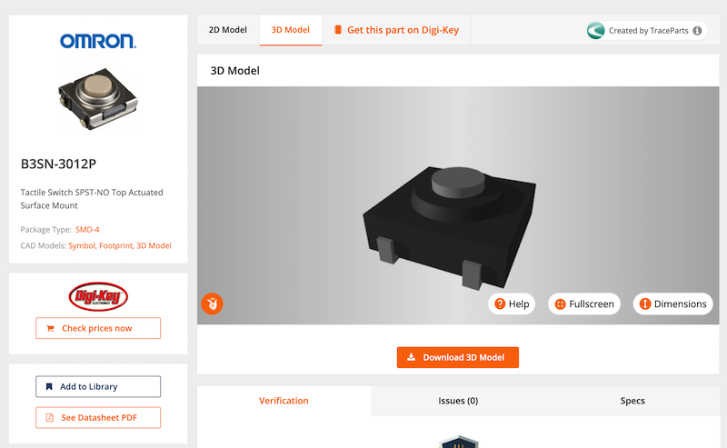
3.1.2 button#
You can import a 3D model of a footprint into Pcbnew, but this is optional.
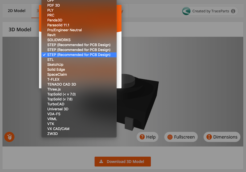
Download 3D model from somewhere. I download it from SnapEDA. Click Download 3D Model.
Select STEP format. Save and unzip it to a current project directory.
In Pcbnew, place a curosr on the footprint of a button. Right click and select Properties….
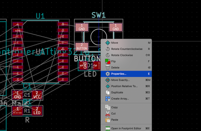
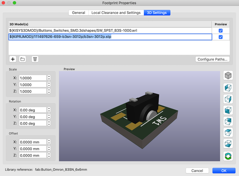
Footprint Property window opens. In `3D Settings@ tab, add a 3D model and navigate to a directory you saved step file.
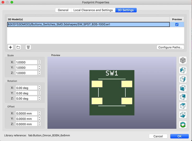
3d model will be imported, but its orientation is not righ.
Rotate the imported 3d component to place on pads right.
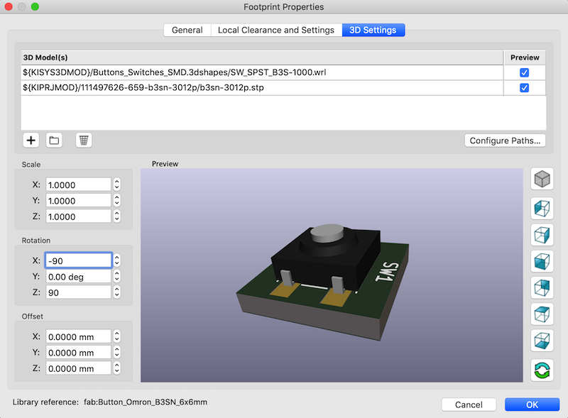
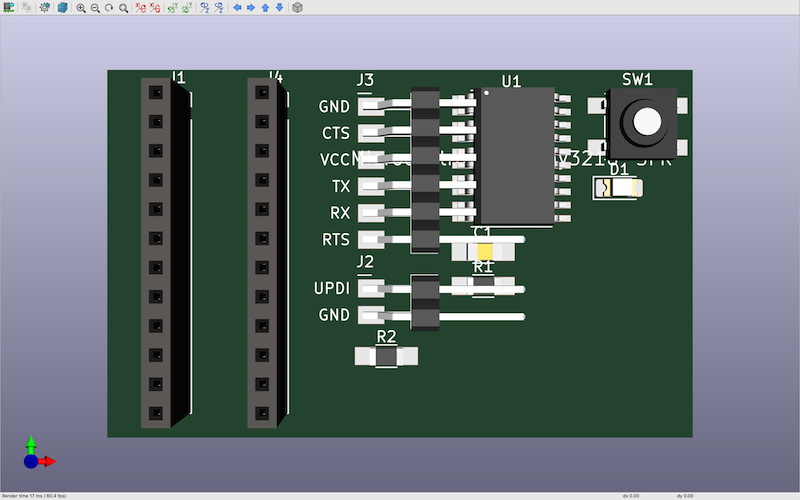
Click OK and go back to 3D viewer. Now a button has nice 3D rendering.
3.2 design PCB#
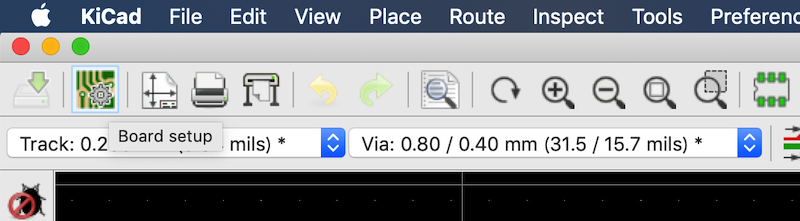
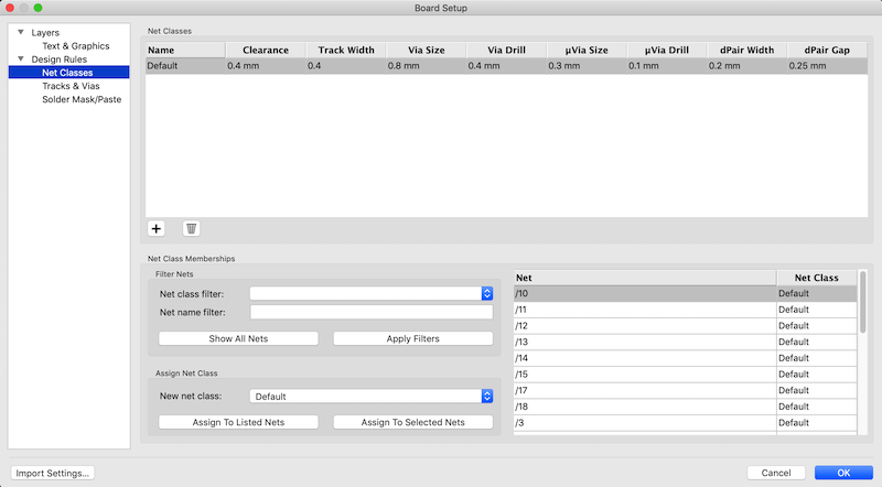
Before working on layout and routing, one thing you have to do is board setup.
In Net Classes, - Clearance: 0.4 mm (assuming that you use 1/64 endmill) - Track width and other values remain unchanged.
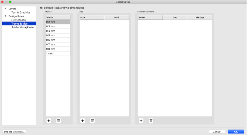
In Tracks & Vias, I setup pre-defined track widths
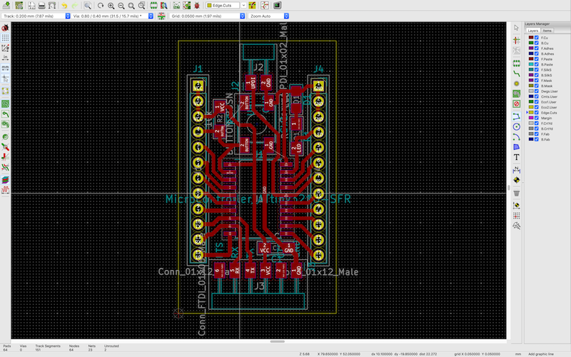
Lay out components as you like.
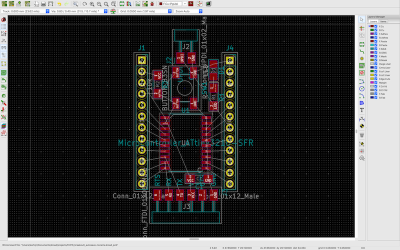
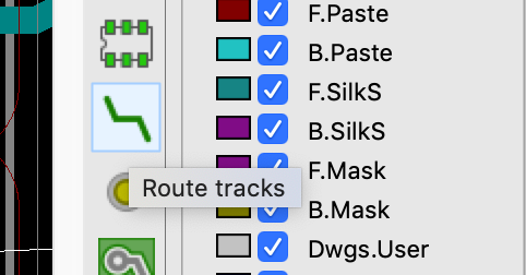
and start wiring components. Click Route tracks icon.
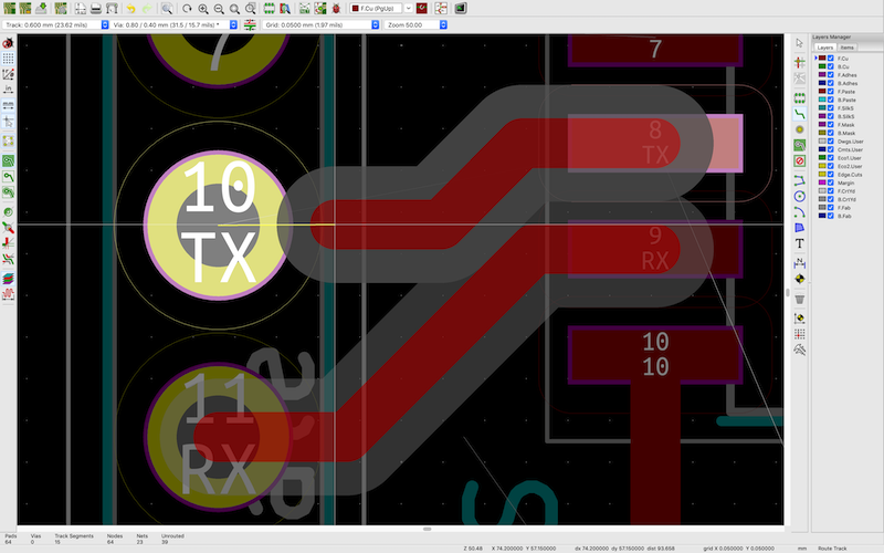
KiCad shows the clearance width(gray area) like below. If other wires are in the way, new routing will push and shove them.
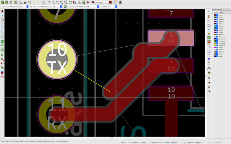
If you setup the clearance 0.1 mm, it looks like this.
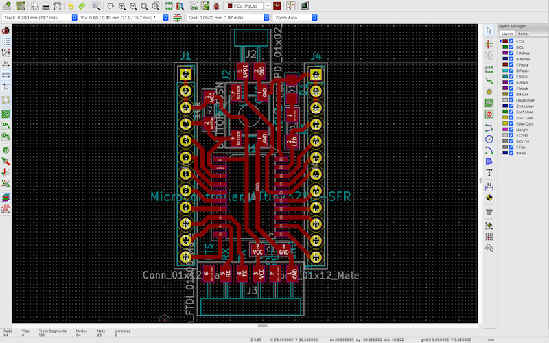
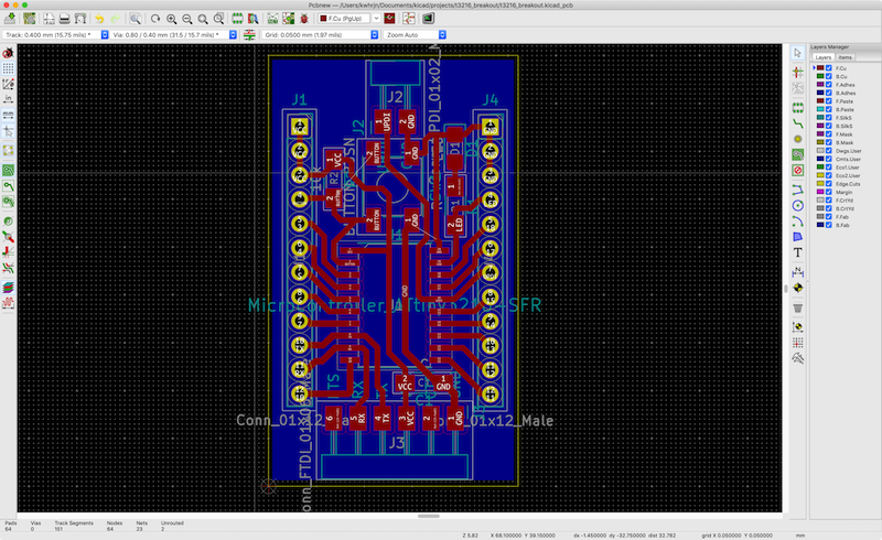
Finish routing as you like.
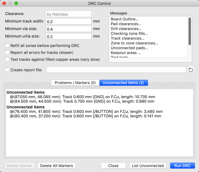
3.3 design rule check(DRC)#
Run DRC(Design Rule Check, click a ladybug icon to open it) to see if your design have problems in the clearance, connection, and so on.
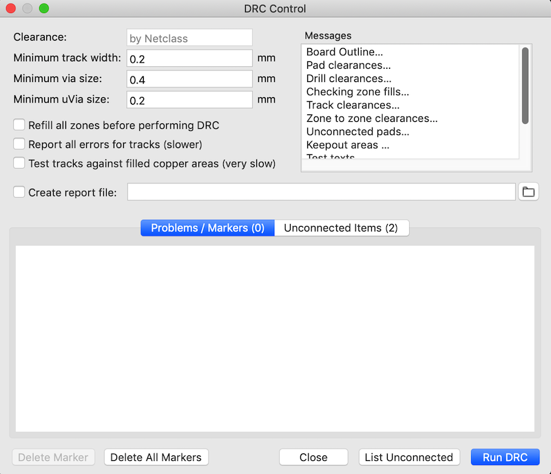
If you have, solve it before going the next step. I can ignore these warnings here.
3.4 export images for milling#
If you want g-code for SRM-20, you’ll need images in a format of SVG or PNG. There are some styles to do this, but here I follow Neil’s.
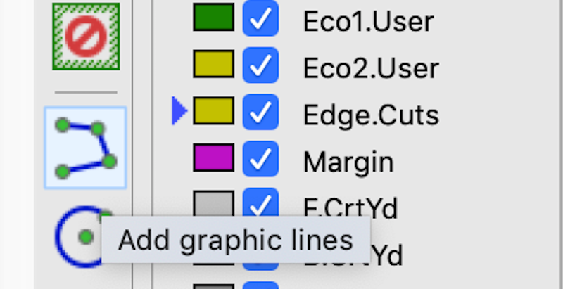
Select Edge.Cuts layer and start add graphic lines to draw a rectangle. It’s going to be a document size.
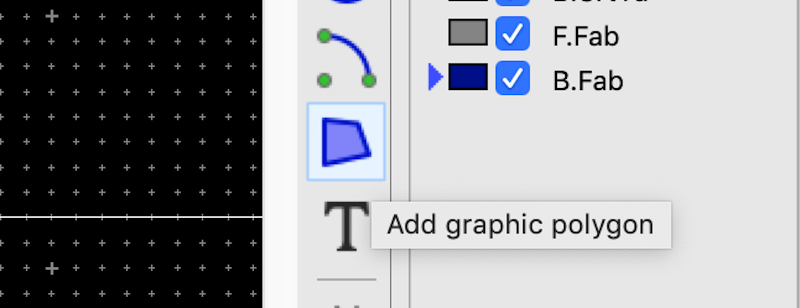
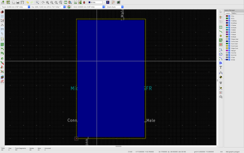
Next, select B.Fab layer, and start adding graphic polygon to draw a cutout geometry of your board.
It’ll turn into a filled geometry.
Back to F.Cu layer then. We’re going to export two images(SVG) for a trace, and a cutout.
File > Export > SVG…
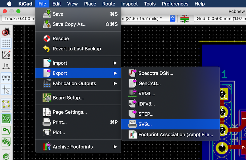
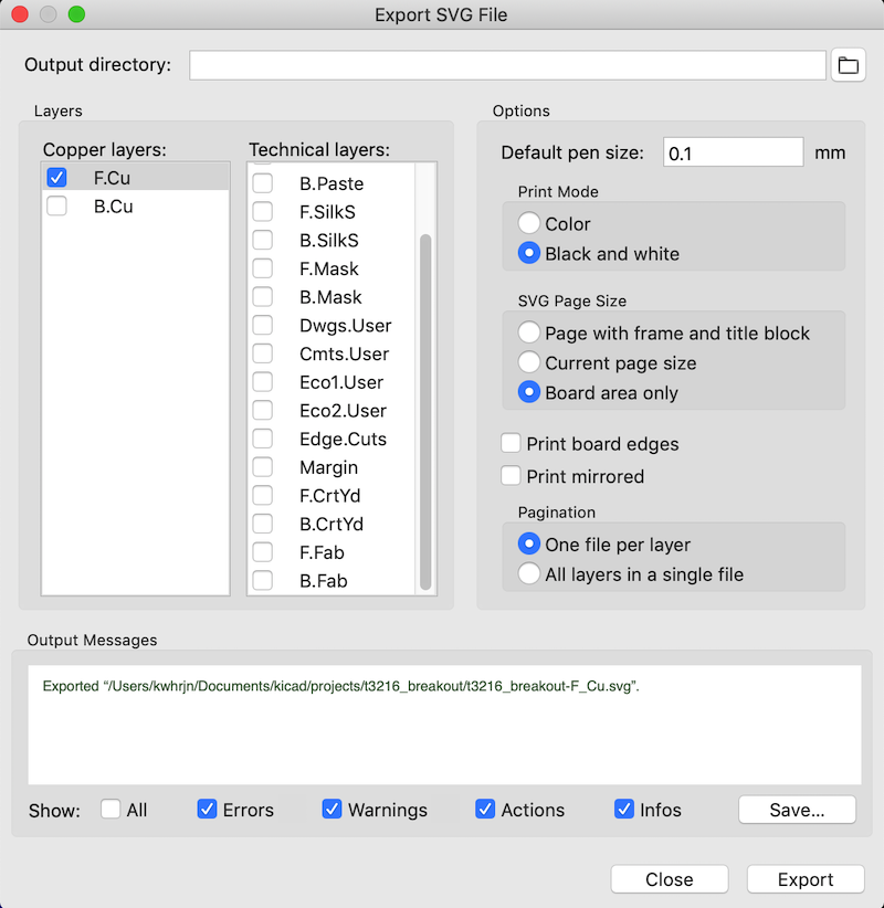
First, for a trace. Select,
- F.Cu in Copper layers
- No in Technical layers
- Print Mode: Black and white
- SVG Page Size: Board area only
- Pagination: One file per layer
then click
Export. A file, “t3216_breakout-F_Cu.svg” will be exported.
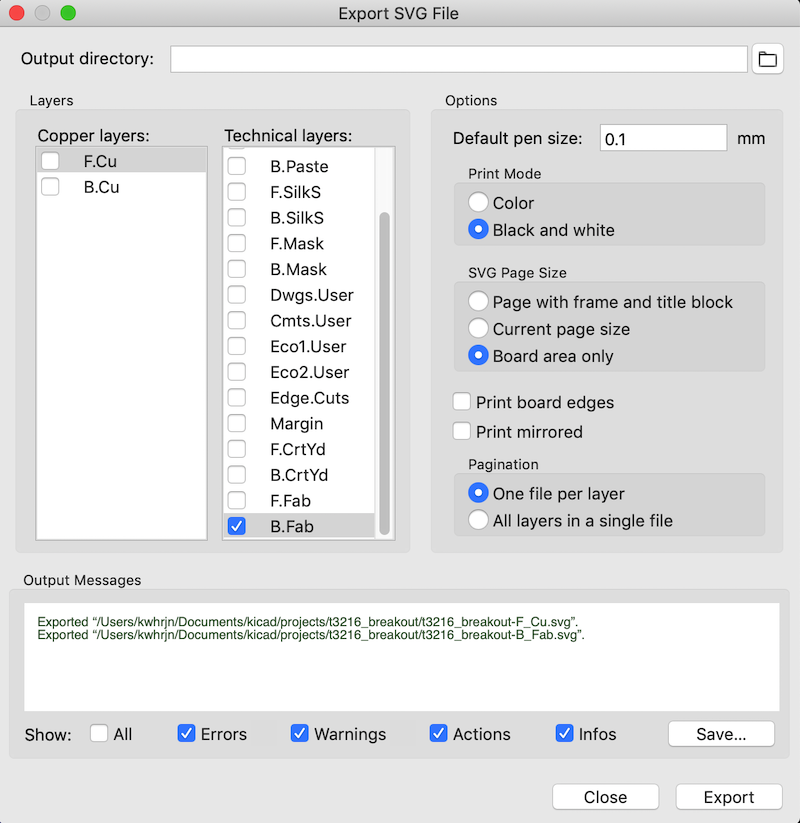
Second for a cutout. Select,
- No in Copper layers
- B.Fab in Technical layers
- others remain the same.
then click
Export. A file, “t3216_breakout-B_Fab.svg” will be exported. Rename it “cutout.svg.”
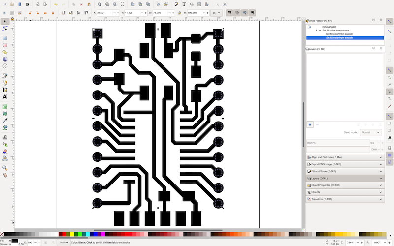
Open t3216_breakout-F_Cu.svg in a vector editor(here I use Inkscacpe).
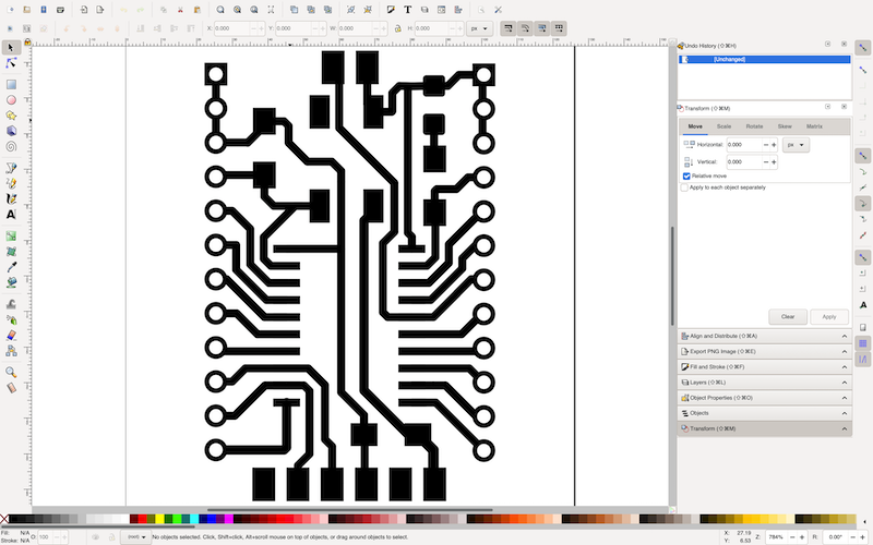
Select all drill holes(temporarily yellow filled circles).
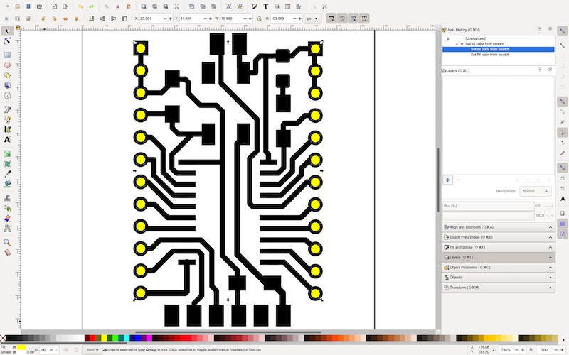
Fill black and save the file as trace.svg.
Edit > Invert Selection
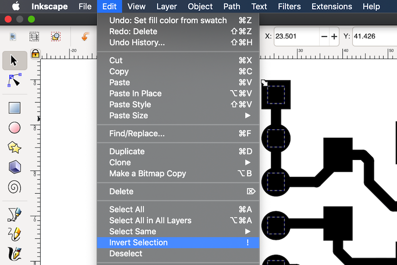
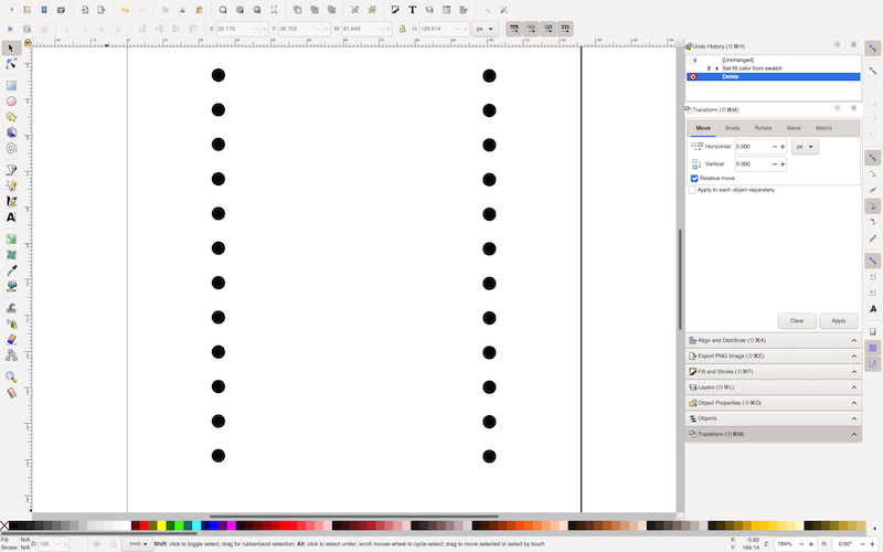
Delete all routing, pads except drill holes, and save it as drill.svg
5. mods settings#
Go mods. Open programs > open server program > machines Roland mill SRM-20 > PCB svg
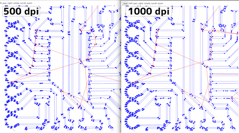
Open trace.svg. In convert SVG image node, invert the image, enter 1000 dpi.
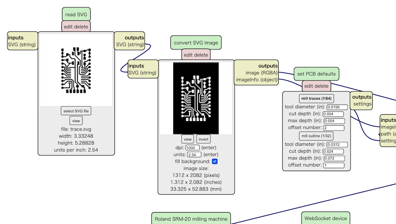
I changed a resolution from 500 dpi to 1000 dpi, because a toolpath from an image with 500 dpi is not smooth enough. See the difference between 500 dpi and 1000 dpi. I used the value in milling drill and cutout.
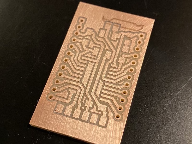
This is the result.
Read this tutorial on how to program tinyAVR as the next step.
design files#
- KiCad project(zip archived)
- Exported SVG files(trace, drills, and cutout)